Meet the Nimble-Fingered Interface of the Future

Microsoft's Kinect, a 3-D camera and software for gaming, has made a big impact since its launch in 2010. Eight million devices were sold in the product's.....

Electronic Implant Dissolves in the Body

Researchers at the University of Illinois at Urbana-Champaign, Tufts University, and ......

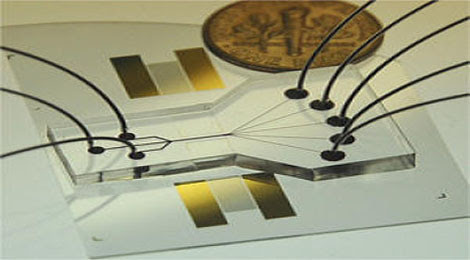
Sorting Chip May Lead to Cell Phone-Sized Medical Labs

The device uses two beams of acoustic -- or sound -- waves to act as acoustic tweezers and sort a continuous flow of cells on a ....

TDK sees hard drive breakthrough in areal density

Perpendicular magnetic recording was an idea that languished for many years, says a TDK technology backgrounder, because the ....

Engineers invent new device that could increase Internet

The device uses the force generated by light to flop a mechanical switch of light on and off at a very high speed........


A Tiny Transistor Hooks Up To Individual Proteins In Human Tears

Wiretapping an enzyme and listening as it unfolds could shed new light on the way proteins work, allowing researchers to monitor structural changes over a longer period of time than was previously possible. To do it, scientists tethered a nanoscale transistor to a molecule found in human tears.


Understanding how proteins fold is a key challenge in biology — making synthetic versions is about much more than their molecular contents. Enzymes change their shapes when they bind their molecular targets, and the way in which this happens has some bearing on the way the proteins work. Researchers have even turned to online games to look for novel folds and structures that could be used in drug discovery and other uses. Biochemists can glimpse these structural changes, but not over long enough time scales to really get a handle on the folding action. Now researchers at the University of California-Irvine say their wiretapping method provides a long-term window into the kinetic behavior of a specific protein.

Yongki Choi and colleagues worked with an enzyme called lysozyme, which is found in human tears and is particularly effective at neutralizing bacteria much larger than itself. They attached the enzyme to a single-walled carbon nanotube, and put the enzyme to work in a reaction assay. The folding and twisting motions induced teeny changes in electrostatic potentials, which the carbon nanotube could detect. Amplifying these signals gave the team a glimpse of the movements the enzyme was making. The team measured these changes in various conditions and over different time scales, they report in their paper, published online today in Science.

"It's just like a stethoscope listening to your heart, except we're listening to a single molecule of protein,” said Philip Collins, a co-author on the paper who typically studies physics and astronomy.
Tiny nanotube field-effect transistors have also been used to listen to cells in action.

The team was able to compare the signals to other measurements made with a technique called single-molecule fluorescence resonance energy transfer spectroscopy. They found the enzymatic actions looked pretty similar between the photon signals and the electron signals — nice confirmation.

This is encouraging because the same technique could be used to study many other molecules, the researchers say.

By Rebecca Boyle
From popsci 

Cloud-Based Quantum Computing Will Allow Secure Calculation on Encrypted Bits

When quantum computers eventually reach larger scales, they’ll probably remain pretty precious resources, locked away in research institutions just like our classical supercomputers. So anyone who wants to perform quantum calculations will likely have to do it in the cloud, remotely accessing a quantum server somewhere else. A new double-blind cryptography method would ensure that these calculations remain secret. It uses the uncertain, unusual nature of quantum mechanics as a double advantage.

 Entangled Qubits Clusters of entangled qubits allow remote quantum computing to be performed on a remote server, while keeping the contents and results hidden.

Imagine you’re a developer and you have some code you’d like to run on a quantum computer. And imagine there’s a quantum computer maker who says you can run your code. But you can’t trust each other — you, the developer, don’t want the computer maker to rip off your great code, and the computer builder doesn’t want you to peep its breakthrough machine. This new system can satisfy both of you. 

Stefanie Barz and colleagues at the University of Vienna’s Center for Quantum Science and Technology prepared an experimental demonstration of a blind computing technique, and tested it with two well-known quantum computing algorithms. Here’s how it would work: You, the developer, prepare some quantum bits, in this case photons that have a polarity (vertical or horizontal) known only to you. Then you would send these to the remote quantum server. The computer would entangle the qubits with even more qubits, using a quantum entangling gate — but the computer wouldn’t know the nature of the entangled states, just that they are in fact entangled. The server is “blind” to the entanglement state, and anyone tapping into the server would be blind, too. 

Imagine the computer tries to snoop on the qubits and see their entanglement, which could then be used to extract the information they carry. You’d be able to tell, because of the laws of quantum mechanics. The cat is both dead and alive until you check whether it’s dead or alive, and then it’s one or the other. If your photon has a specific state, you’d be able to tell that it was spied upon.

Back to the entangled bits. The actual information processing takes place via a sequence of measurements on your qubits. These measurements would be directed by you, based on the particular states of each qubit (which, again, only you know). The quantum server would run the measurements and report the results to you. This is called measurement-based quantum computation. Then you’d be able to interpret the results, based on your knowledge of the qubits’ initial states. To the computer — or any interceptor — the whole thing would look utterly random. 

Since you know the entangled state on which the measurements were made, you can be certain whether the server really was a quantum computer. And you wouldn’t have to disclose your algorithm, the input or even the output — it’s perfectly secure, the researchers write in their paper, published online today in Science.

Blind quantum computation is more secure than classical blind computation, which relies on tactics like the backward factoring of prime numbers, said Vlatko Vedral, a researcher at the University of Oxford who wrote a Perspective piece explaining this finding.

“The double blindness is guaranteed by the laws of quantum physics, instead of the assumed difficulty of of computational tasks as in classical physics,” Vedral writes.

The Vienna team argues their simulation is a potentially useful technique for future cloud-based quantum computing networks.

“Our experiment is a step toward unconditionally secure quantum computing in a client-server environment where the client’s entire computation remains hidden, a functionality not known to be achievable in the classical world,” they write. 

By Rebecca Boyle
From popsci

Physicists cool semiconductor by laser light

 The experiments themselves are carried out in this vacuum chamber. When the laser light hits the membrane, some of the light is reflected and some is absorbed and leads to a small heating of the membrane. The reflected light is reflected back again via a mirror in the experiment so that the light flies back and forth in this space and forms optical resonator (cavity). Changing the distance between the membrane and the mirror leads to a complex and fascinating interplay between the movement of the membrane, the properties of the semiconductor and the optical resonances and you can control the system so as to cool the temperature of the membrane fluctuations.


"In experiments, we have succeeded in achieving a new and efficient cooling of a solid material by using lasers. We have produced a semiconductor membrane with a thickness of 160 nanometers and an unprecedented surface area of 1 by 1 millimeter. In the experiments, we let the membrane interact with the laser light in such a way that its mechanical movements affected the light that hit it. We carefully examined the physics and discovered that a certain oscillation mode of the membrane cooled from room temperature down to minus 269 degrees C, which was a result of the complex and fascinating interplay between the movement of the membrane, the properties of the semiconductor and the optical resonances," explains Koji Usami, associate professor at Quantop at the Niels Bohr Institute.

From gas to solid
Laser cooling of atoms has been practiced for several years in experiments in the quantum optical laboratories of the Quantop research group at the Niels Bohr Institute. Here researchers have cooled gas clouds of cesium atoms down to near absolute zero, minus 273 degrees C, using focused lasers and have created entanglement between two atomic systems. The atomic spin becomes entangled and the two gas clouds have a kind of link, which is due to quantum mechanics. Using quantum optical techniques, they have measured the quantum fluctuations of the atomic spin.

"For some time we have wanted to examine how far you can extend the limits of quantum mechanics – does it also apply to macroscopic materials? It would mean entirely new possibilities for what is called optomechanics, which is the interaction between optical radiation, i.e. light, and a mechanical motion," explains Professor Eugene Polzik, head of the Center of Excellence Quantop at the Niels Bohr Institute at the University of Copenhagen.
But they had to find the right material to work with. 

 Koji Usami shows the holder with the semiconductor nanomembrane. The holder measures about one cm for each link, while the nanomembrane itself has a surface area of 1 times 1 millimeter and a thickness of 160 nanometers.

In 2009, Peter Lodahl (who is today a professor and head of the Quantum Photonic research group at the Niels Bohr Institute) gave a lecture at the Niels Bohr Institute, where he showed a special photonic crystal membrane that was made of the semiconducting material gallium arsenide (GaAs). Eugene Polzik immediately thought that this nanomembrane had many advantageous electronic and optical properties and he suggested to Peter Lodahl's group that they use this kind of membrane for experiments with optomechanics. But this required quite specific dimensions and after a year of trying they managed to make a suitable one.

"We managed to produce a nanomembrane that is only 160 nanometers thick and with an area of more than 1 square millimetre. The size is enormous, which no one thought it was possible to produce," explains Assistant Professor Søren Stobbe, who also works at the Niels Bohr Institute.

 The experiments are carried out by Koji Usami here in the Quantop laboratories at the Niels Bohr Institute. The laser light that hits the semiconducting nanomembrane is controlled with a forest of mirrors.

Basis for new research
Now a foundation had been created for being able to reconcile quantum mechanics with macroscopic materials to explore the optomechanical effects.

Koji Usami explains that in the experiment they shine the laser light onto the nanomembrane in a vacuum chamber. When the laser light hits the semiconductor membrane, some of the light is reflected and the light is reflected back again via a mirror in the experiment so that the light flies back and forth in this space and forms an optical resonator. Some of the light is absorbed by the membrane and releases free electrons. The electrons decay and thereby heat the membrane and this gives a thermal expansion. In this way the distance between the membrane and the mirror is constantly changed in the form of a fluctuation.

"Changing the distance between the membrane and the mirror leads to a complex and fascinating interplay between the movement of the membrane, the properties of the semiconductor and the optical resonances and you can control the system so as to cool the temperature of the membrane fluctuations. This is a new optomechanical mechanism, which is central to the new discovery. The paradox is that even though the membrane as a whole is getting a little bit warmer, the membrane is cooled at a certain oscillation and the cooling can be controlled with laser light. So it is cooling by warming! We managed to cool the membrane fluctuations to minus 269 degrees C", Koji Usami explains.

"The potential of optomechanics could, for example, pave the way for cooling components in quantum computers. Efficient cooling of mechanical fluctuations of semiconducting nanomembranes by means of light could also lead to the development of new sensors for electric current and mechanical forces. Such cooling in some cases could replace expensive cryogenic cooling, which is used today and could result in extremely sensitive sensors that are only limited by quantum fluctuations," says Professor Eugene Polzik.
Provided by University of Copenhagen

From physorg

Cambridge team uses solar cells in OLED screen to power smartphones

A team of researchers at the University of Cambridge are getting closer. Their idea is to harvest energy from wasted light in an OLED display. They are working on technology where users will not need to plug in their smartphones for recharging at least as often. In their project, an OLED screen uses solar cells to absorb scattered and wasted light, sending it back into the screen. 

 A thin-film system harvests energy from wasted light in an OLED display.

IEEE Fellow Arokia Nathan along with the Cambridge team have developed a prototype device that converts ambient light into electricity. Solar cells used in the prototype are made of thin film hydrogenated amorphous silicon, within the smartphone screen. 

Only around 36 percent of the light produced by an OLED display is projected forwards; the rest escapes around the edges, in the form of scatter and bleeding from the edges. The researchers worked on a solution where they could harvest what’s lost by installing photovoltaic cells on the back and sides of OLED screens to capture the loss. 

They also worked out a solution—a thin-film transistor circuit--to even out the voltage spikes produced by the solar cells, as fluctuations in the voltage provided by the solar cell could damage the phone’s battery. The device captures both ambient light and the otherwise wasted screen light leaking around the edges.

According to reports, the team worked with the energy group at Cambridge's Centre for Advanced Photonics and Electronics to integrate a thin-film supercapacitor for intermediate energy storage. 

The end result is a system that makes use of photovoltaics, transistors, and supercapacitor. The system would achieve an efficiency of 11 percent and peak efficiency, 18 percent.

The numbers, for the smartphone user, would promise at least less strain on their battery. The Cambridge team’s effort is not promising “never-again” recharging but an ability for the user to save a fraction of power.

More work is ahead. The team is exploring different circuit designs and materials with the aim of increasing the energy harvesting system’s efficiency. Nathan has said other energy scavenging schemes such as MEMS based kinetic energy harvesting may bring improvements.

By Nancy Owano
From physorg.
 

Metal Oxide Simulations Could Help Green Technology

 Computer simulations show that metal oxides in water go through many short-lived shapes and structures.

Their work appears in the current issue of the journal Nature Materials.

The new paradigm could lead to a better understanding of corrosion and how toxic minerals leach from rocks and soil. It could also help in the development of "green" technology: new types of batteries, for example, or catalysts for splitting water to produce hydrogen fuel.

"This is a global change in how people should view these processes," said William Casey, UC Davis professor of chemistry and co-author of the study with James Rustad, a former geology professor at UC Davis who now works as a scientist at Corning Inc. in New York.

Previously, when studying the interactions of water with clusters of metal oxides, researchers tried to pick and study individual atoms to assess their reactivity. But "none of it really made sense," Rustad said.

Using computer simulations developed by Rustad, and comparing the resulting animations with lab experiments by Casey, the two found that the behavior of an atom on the surface of the cluster can be affected by an atom some distance away.

Instead of moving through a sequence of transitional forms, as had been assumed, metal oxides interacting with water fall into a variety of "metastable states" -- short-lived intermediates, the researchers found.

For example, in one of Rustad's animations, a water molecule approaches an oxygen atom on the surface of a cluster. The oxygen suddenly pulls away from another atom binding it into the middle of the cluster and leaps to the water molecule. Then the structure collapses back into place, ejecting a spare oxygen atom and incorporating the new one.

From sciencedaily

Almost Perfect: Researcher Nears Creation of Superlens

No one has yet made a superlens, also known as a perfect lens, though people are trying. Optical lenses are limited by the nature of light, the so-called diffraction limit, so even the best won't usually let us see objects smaller than 200 nanometers across, about the size of the smallest bacterium. Scanning electron microscopes can capture objects that are much smaller, about a nanometer wide, but they are expensive, heavy, and, at the size of a large desk, not very portable.

 In this illustration of Durdu Guney's theoretical metamaterial, the colors show magnetic fields generated by plasmons. The black arrows show the direction of electrical current in metallic layers, and the numbers indicate current loops that contribute to negative refraction.

To build a superlens, you need metamaterials: artificial materials with properties not seen in nature. Scientists are beginning to fabricate metamaterials in their quest to make real seemingly magical phenomena like invisibility cloaks, quantum levitation -- and superlenses.

Now Guney, an assistant professor of electrical and computer engineering at Michigan Technological University, has taken a major step toward creating superlens that could use visible light to see objects as small as 100 nanometers across.

The secret lies in plasmons, charge oscillations near the surface of thin metal films that combine with special nanostructures. When excited by an electromagnetic field, they gather light waves from an object and refract it in a way not seen in nature called negative refraction. This lets the lens overcomes the diffraction limit. And, in the case of Guney's model, it could allow us to see objects smaller than 1/1,000th the width of a human hair.

Other researchers have also been able to sidestep the diffraction limit, but not throughout the entire spectrum of visible light. Guney's model showed how metamaterials might be "stretched" to refract light waves from the infrared all the way past visible light and into the ultraviolet spectrum.

Making these superlenses would be relatively inexpensive, which is why they might find their way into cell phones. But there would be other uses as well, says Guney.

"It could also be applied to lithography," the microfabrication process used in electronics manufacturing. "The lens determines the feature size you can make, and by replacing an old lens with this superlens, you could make smaller features at a lower cost. You could make devices as small as you like."

Computer chips are made using UV lasers, which are expensive and difficult to build. "With this superlens, you could use a red laser, like the pointers everyone uses, and have simple, cheap machines, just by changing the lens."

What excites Guney the most, however, is that a cheap, accessible superlens could open our collective eyes to worlds previously known only to a very few.

"The public's access to high-powered microscopes is negligible," he says. "With superlenses, everybody could be a scientist. People could put their cells on Facebook. It might just inspire society's scientific soul."

Guney and graduate student Muhammad Aslam published an article on their work, "Surface Plasmon Diven Scalable Low-Loss Negative-Index Metamaterial in the visible spectrum," in Physical Review B, volume 84, issue 19.0

From sciencedaily

Umbilical Cord Stem Cells Converted Into Brain Support Cells

"This is the first time this has been done with non-embryonic stem cells," says James Hickman, a University of Central Florida bioengineer and leader of the research group, whose accomplishment is described in the Jan. 18 issue of the journal ACS Chemical Neuroscience.

 James Hickman.

"We're very excited about where this could lead because it overcomes many of the obstacles present with embryonic stem cells."

Stem cells from umbilical cords do not pose an ethical dilemma because the cells come from a source that would otherwise be discarded. Another major benefit is that umbilical cells generally have not been found to cause immune reactions, which would simplify their potential use in medical treatments.

The pharmaceutical company Geron, based in Menlo Park, Calif., developed a treatment for spinal cord repair based on embryonic stem cells, but it took the company 18 months to get approval from the FDA for human trials due in large part to the ethical and public concerns tied to human embryonic stem cell research. This and other problems recently led to the company shutting down its embryonic stem cell division, highlighting the need for other alternatives.

Sensitive Cells
The main challenge in working with stem cells is figuring out the chemical or other triggers that will convince them to convert into a desired cell type. When the new paper's lead author, Hedvika Davis, a postdoctoral researcher in Hickman's lab, set out to transform umbilical stem cells into oligodendrocytes -- critical structural cells that insulate nerves in the brain and spinal cord -- she looked for clues from past research.

Davis learned that other research groups had found components on oligodendrocytes that bind with the hormone norephinephrine, suggesting the cells normally interact with this chemical and that it might be one of the factors that stimulates their production. So, she decided this would be a good starting point.

In early tests, she found that norepinephrine, along with other stem cell growth promoters, caused the umbilical stem cells to convert, or differentiate, into oligodendrocytes. However, that conversion only went so far. The cells grew but then stopped short of reaching a level similar to what's found in the human nervous system.

Davis decided that, in addition to chemistry, the physical environment might be critical.
To more closely approximate the physical restrictions cells face in the body, Davis set up a more confined, three-dimensional environment, growing cells on top of a microscope slide, but with a glass slide above them. Only after making this change, and while still providing the norephinphrine and other chemicals, would the cells fully mature into oligodendrocytes.
"We realized that the stem cells are very sensitive to environmental conditions," Davis said.

Medical Potential
This growth of oligodendrocytes, while crucial, is only a first step to potential medical treatments. There are two main options the group hopes to pursue through further research. The first is that the cells could be injected into the body at the point of a spinal cord injury to promote repair.

Another intriguing possibility for the Hickman team's work relates to multiple sclerosis and similar conditions. "Multiple sclerosis is one of the holy grails for this kind of research," said Hickman, whose group is collaborating with Stephen Lambert at UCF's medical school, another of the paper's authors.

Oligodendrocytes produce myelin, which insulates nerve cells, making it possible for them to conduct the electrical signals that guide movement and other functions. Loss of myelin leads to multiple sclerosis and other related conditions such as diabetic neuropathy.

The injection of new, healthy oligodendrocytes might improve the condition of patients suffering from such diseases. The teams are also hoping to develop the techniques needed to grow oligodendrocytes in the lab to use as a model system both for better understanding the loss and restoration of myelin and for testing potential new treatments.

"We want to do both," Hickman said. "We want to use a model system to understand what's going on and also to look for possible therapies to repair some of the damage, and we think there is great potential in both directions."

Besides Hickman and Davis, the other authors on the paper were Xiufang Guo, Stephen Lambert, and Maria Stancescu, all from the University of Central Florida.

From sciencedaily

New Process Makes Heat-Harvesting Materials Cheaply

High-efficiency thermoelectric materials could lead to new types of cooling systems, and new ways to scavenge waste heat for electricity. Researchers at Rensselaer Polytechnic Institute in Troy, New York, have now developed an easy, inexpensive process to make such materials.

The materials made by the RPI team already perform as well as those on the market, and the new process, which involves zapping chemicals in a microwave oven, offers room for improvement. "We haven't even optimized the process yet," says Ganpati Ramanath, a materials science and engineering professor at RPI. "We're confident that we can increase the efficiency further."

 Cooked to order: Zapping raw materials in a microwave oven and drying the resulting solution produces a black powder (top) made of hexagonal bismuth telluride nanoplates (bottom).

Thermoelectric materials convert heat into electricity, and vice versa. They are used in niche applications such as power generation on spacecraft and temperature-controlled car seats. If they were cheaper and more efficient, they could perhaps be used to make lightweight refrigerators, cooling systems for computer chips and buildings, and for using car exhaust heat to power electronics such as headlights and the radio. 

Good thermoelectrics need to conduct electricity well but heat poorly. One way to boost the heat-transfer efficiency of such materials is to give them nanoscale features that block the flow of heat without restricting electric current.

Researchers have made nanostructured materials by breaking up crystals into fine powder. But this process is energy intensive and only results in high-efficiency p-type thermoelectric materials—the kind rich in positively charged particles called holes. But both p-type and n-type materials (which have an abundance of electrons) are needed for practical devices. 

"We've shown that we can make both p- and n-type materials, and we can do this very scalably and more cost-effectively," Ramanath says. "We can make gram quantities in minutes." 

Ramanath and his colleagues make a solution from raw materials such as tellurium and bismuth chloride in an organic solvent, and put it in a domestic microwave oven for two to three minutes. They get a solution containing hexagonal nanoplates, which they press together and heat to make nanopellets. By using a solvent containing sulfur, the researchers get sulfur-doped nanoplates that are n-type. 

The technique, presented in a Nature Materials paper posted online last week, makes p-type materials that are as efficient as the best ones on the market, while the n-type materials are at least 25 percent more efficient. One of the biggest commercial thermoelectric device manufacturers is now interested in adopting the new materials and process.

"This is the first nanostructured n-type mat with a high [efficiency] value," says John Badding, a professor of chemistry at Penn State University.

The key breakthrough of the RPI work, according to Badding, is that the researchers are building the nanostructured materials from the bottom up using chemistry. This means they can fine-tune the properties of the building blocks and their assembly to improve the material's properties. "The way they're making the material is a big deal," he says. "The hope is that in the future, this type of approach could lead to better [efficiency]."

By Prachi Patel
From Technology Review

Magnetic Memory Miniaturized to Just 12 Atoms

The smallest magnetic-memory bit ever made—an aggregation of just 12 iron atoms created by researchers at IBM—shows the ultimate limits of future data-storage systems. 

The magnetic memory elements don't work in the same way that today's hard drives work, and, in theory, they can be much smaller without becoming unstable. Data-storage arrays made from these atomic bits would be about 100 times denser than anything that can be built today. But the 12 atoms making up each bit must be painstakingly assembled using an expensive and complex microscope, and the bits can hold data for only a few hours and at low temperatures approaching absolute zero, so the miniscule memory elements won't be found in consumer devices anytime soon.

 Let's get small: This scanning tunneling microscope image shows a group of 12 iron atoms, the smallest magnetic memory bit ever made.

As the semiconductor industry bumps up against the limits of scaling by making memory and computation devices ever smaller, the IBM Almaden research group, led by Andreas Heinrich, is working from the other end, building computing elements atom-by-atom in the lab. 

The necessary technology for large-scale manufacturing at the single-atom scale doesn't exist yet. Today, says Heinrich, the question is, "What is it you would want to build on the scale of atoms for data storage and computation, in the distant future?"

As engineers miniaturize conventional devices, they're finding that quantum physics, which never had to be accounted for in the past, makes devices less stable. As conventional magnetic memory bits are miniaturized, for example, each bit's magnetic field begins to affect its neighbors', weakening each bit's ability to hold on to a 1 or a 0. 

The IBM researchers found that it was possible to sidestep this problem by using groups of atoms that display a different kind of magnetism. The key, says Heinrich, is the magnetic spin of each individual atom. 

In conventional magnets, whether they're found holding up a note on the refrigerator or in a data-storage array, the magnetic spins of the atoms are aligned. It's this alignment that leads to instability when magnetic-memory elements are miniaturized. The IBM researchers made their tiny memory elements by lining up iron atoms whose spins were counter-aligned.

The researchers both constructed and wrote data to the tiny memory elements using a scanning tunneling microscope, a device developed at IBM Zürich in 1981. This microscope has a very thin conducting probe that can be used to image a surface and push individual atoms around. 

Heinrich says his team found it could make antiferromagnetic memory using fewer than 12 atoms, but these were less stable. With 12 atoms, the memory elements obey classical physics, and the read-and-write pulses applied through the microscope probe are similar to those used in today's hard drives. This research is described today in the journal Science.

Any realistic nonvolatile data storage technology has to be able to hold onto the data for 10 years at temperatures well over room temperature, says Victor Zhirnov, a research scientist at the Semiconductor Research Corporation, who was not involved with the work. The IBM bits can hold onto a 1 or a 0 for just a few hours, and only at very low temperatures, but Heinrich says it should be possible to increase their stability for operation at more realistic temperatures by using 150 atoms per bit rather than 12—still a miniscule number compared to existing forms of memory.

However, making a realistic technology was not the aim of the current work, says Heinrich. His aim is to explore whether other kinds of computing elements can be made from a few atoms, perhaps by embracing quantum. "We have to have the foresight not to worry about the next step, but to jump to something potentially revolutionary," he says. 

By Katherine Bourzac
From Technology Review